COMPUTER ARCHITECTURE AND HARDWARE MAINTENANCE:-
CPU ORGANIZATION:-
Generally CPU has seven general registers. Register organization show how registers are selected and how data flow between register and ALU. A decoder is used to select a particular register.The output of each register is connected to two multiplexers to form the two buses A and B. The selection lines in each multiplexer select the input data for the particular bus.
The A and B buses form the two inputs of an ALU.The operation select lines decide the micro operation to be performed by ALU. The result of the micro operation is available at the output bus. The output bus connected to the inputs of all registers, thus by selecting a destination register it is possible to store the result in it.
A bus organization for seven CPU register

To perform the operation R3 = R1+R2 We have to provide the following binary selection variable to the select inputs.EXAMPLE:
- SEL A : 001 -To place the contents of R1 into bus A.
- SEL B : 010 – to place the contents of R2 into bus B
- SEL OPR : 10010 – to perform the arithmetic addition A+B
- SEL REG or SEL D : 011 – to place the result available on the output bus in R3.
Register and multiplexer input selection code
| Binary code | SELA | SELB | SELD or SELREG |
| 000 | Input | Input | — |
| 001 | R1 | R1 | R1 |
| 010 | R2 | R2 | R2 |
| 011 | R3 | R3 | R3 |
| 100 | R4 | R4 | R4 |
| 101 | R5 | R5 | R5 |
| 110 | R6 | R6 | R6 |
| 111 | R7 | R7 | R7 |
Operation with symbol
| Operation selection code | Operation | symbol |
| 0000 | Transfer A | TSFA |
| 0001 | Increment A | INC A |
| 0010 | A+B | ADD |
| 0011 | A-B | SUB |
| 0100 | Decrement A | DEC |
| 0101 | A AND B | AND |
| 0110 | A OR B | OR |
| 0111 | A XOR B | XOR |
| 1000 | Complement A | COMA |
| 1001 | Shift right A | SHR |
| 1010 | Shift left A | SHL |
What is CONTROL WORD?
- The combined value of a binary selection inputs specifies the control word.
- It consist of four fields SELA,SELB,and SELD or SELREG contains three bit each and SELOPR field contains four bits thus the total bits in the control word are 13-bits.
| SEL A | SELB | SELREG OR SELD | SELOPR |
FORMATE OF CONTROL WORD
- The three bit of SELA select a source registers of the a input of the ALU.
- The three bits of SELB select a source registers of the b input of the ALU.
- The three bits of SELED or SELREG select a destination register using the decoder.
- The four bits of SELOPR select the operation to be performed by ALU.
CONTROL WORD FOR OPERATION R2 = R1+R3
| SEL A | SEL B | SEL D OR SELREG | SELOPR |
| 001 | 011 | 010 | 0010 |
Note: Control words for all micro operation are stored in the control memory
Example:
| MICROOPERATION | SEL A | SEL B | SEL D OR SELREG | SELOPR | CONTROL WORD | |||
| R2 = R1+R3 | R1 | R3 | R2 | ADD | 001 | 011 | 010 | 0010 |
STACK ORGANIZATION:-
To organize data we need some data structure like array stack link list etc. Program have different type of data , it can be stored in computer memory or cpu registers. data type who support different type of data and as well as easy manipulation.Stack fulfill these requirement. So we need stack.
What is Stack:
- A stack is a list of data elements, usually words or bytes, with the accessing restriction that the element can be added or removed at one end of the list only. This end is called the top of the stack and the other end is called the bottom of the stack.
- Stack work on LIFO concept.
- Placing new data element called PUSH
- Removing the top data element called POP.
How computer uses stack?
- Stack can be part of register unit or memory unit with a register that holds the address for the stack.
- Part of register array or memory used for stack is called stack area.
- Register which used to hold the address of stack is called stack pointer.
- The value in the stack pointer always points at the top data element in the stack.
Register stack::
- Four element store in stack.
- The data element 50 is top of stack, therefore the content Of SP is now 4.
- The stack pointer is a 5 bit register, because 2^5=32.
- Initialy it is clear to 0 and stack is said to be empty.
- When data element is pushed on the stack,SP incremented.

Memory stack ::
- Operation of memory stack is exactly similar to register stack. However it is implemented using computer memory instead of CPU register array.
- Memory stack has an advantage of large size but the operation on it is slower than that of register stack.
- This is because register stack is internal to the CPU and does not need any memory access.

Instruction Formats (Zero, One, Two and Three Address Instruction)
Computer perform task on the basis of instruction provided. A instruction in computer comprises of groups called fields. These field contains different information as for computers every thing is in 0 and 1 so each field has different significance on the basis of which a CPU decide what so perform. The most common fields are:
- Operation field which specifies the operation to be performed like addition.
- Address field which contain the location of operand, i.e., register or memory location.
- Mode field which specifies how operand is to be founded.
A instruction is of various length depending upon the number of addresses it contain. Generally CPU organization are of three types on the basis of number of address fields:
- Single Accumulator organization
- General register organization
- Stack organization
In first organization operation is done involving a special register called accumulator. In second on multiple registers are used for the computation purpose. In third organization the work on stack basis operation due to which it does not contain any address field. It is not necessary that only a single organization is applied a blend of various organization is mostly what we see generally.
On the basis of number of address instruction are classified as:
Note that we will use X = (A+B)*(C+D) expression to showcase the procedure.
- Zero Address Instructions –
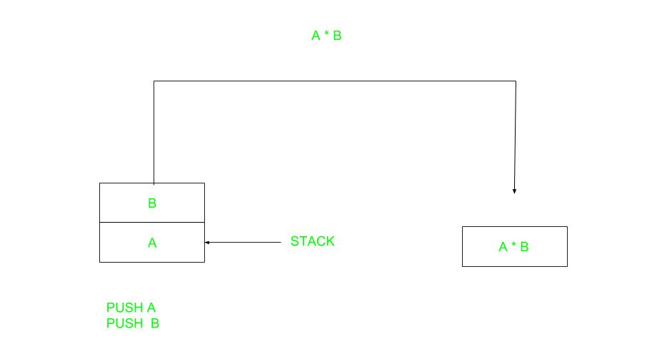 A stack based computer do not use address field in instruction.To evaluate a expression first it is converted to revere Polish Notation i.e. Post fix Notation.
Expression: X = (A+B)*(C+D) Postfixed : X = AB+CD+* TOP means top of stack M[X] is any memory location
PUSH A TOP = A PUSH B TOP = B ADD TOP = A+B PUSH C TOP = C PUSH D TOP = D ADD TOP = C+D MUL TOP = (C+D)*(A+B) POP X M[X] = TOP - One Address Instructions –
This use a implied ACCUMULATOR register for data manipulation.One operand is in accumulator and other is in register or memory location.Implied means that the CPU already know that one operand is in accumulator so there is no need to specify it.
Expression: X = (A+B)*(C+D) AC is accumulator M[] is any memory location M[T] is temporary location
| LOAD | A | AC = M[A] |
| ADD | B | AC = AC + M[B] |
| STORE | T | M[T] = AC |
| LOAD | C | AC = M[C] |
| ADD | D | AC = AC + M[D] |
| MUL | T | AC = AC * M[T] |
| STORE | X | M[X] = AC |
- Two Address Instructions –
This is common in commercial computers.Here two address can be specified in the instruction.Unlike earlier in one address instruction the result was stored in accumulator here result cab be stored at different location rather than just accumulator, but require more number of bit to represent address.
Here destination address can also contain operand.Expression: X = (A+B)*(C+D) R1, R2 are registers M[] is any memory location
MOV R1, A R1 = M[A] ADD R1, B R1 = R1 + M[B] MOV R2, C R2 = C ADD R2, D R2 = R2 + D MUL R1, R2 R1 = R1 * R2 MOV X, R1 M[X] = R1
Three Address Instructions –
This has three address field to specify a register or a memory location. Program created are much short in size but number of bits per instruction increase. These instructions make creation of program much easier but it does not mean that program will run much faster because now instruction only contain more information but each micro operation (changing content of register, loading address in address bus etc.) will be performed in one cycle only.
This has three address field to specify a register or a memory location. Program created are much short in size but number of bits per instruction increase. These instructions make creation of program much easier but it does not mean that program will run much faster because now instruction only contain more information but each micro operation (changing content of register, loading address in address bus etc.) will be performed in one cycle only.
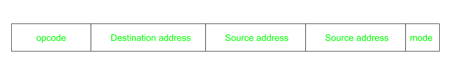
Expression: X = (A+B)*(C+D) R1, R2 are registers M[] is any memory location
| ADD | R1, A, B | R1 = M[A] + M[B] |
| ADD | R2, C, D | R2 = M[C] + M[D] |
| MUL | X, R1, R2 | M[X] = R1 * R2 |
RISC Instructions:-
The advantages of a reduced instruction set computer (RISC) architecture are
explained in Sec. 8-8. The instruction set of a typical RISC processor is restricted
260 CHAPTER EIGHT Central Processing Unit
to the use of load and store instructions when communicating between memory and CPU. All other instructions are executed within the registers of the
CPU without referring to memory. A program for a RISC-type CPU consists
of LOAD and STORE instructions that have one memory and one register
address, and computational-type instructions that have three addresses with
all three specifying processor registers. The following is a program to evaluate
X = (A + B) • (C + D).
LOAD R 1 , A R 1 <– M[A ]
LOAD R 2 , B R 2 <– M[B]
LOAD R 3 , c R3 <– M[C]
LOAD RL; , D RL; <– M[D]
ADD R 1 , R 1 , R2 R 1 <– R1 + R2
ADD R 3 , R 3 , R2 R 3 <– R3 + RL;
MOL R 1 , R 1 , R3 R 1 <– R 1 • R 3
STORE X, R1 M[X] <– R1
The load instructions transfer the operands from memory to CPU registers.
The add and multiply operations are executed with data in the registers
without accessing memory. The result of the computations is then stored in
memory with a store instruction
Addressing Modes
Addressing Modes– The term addressing modes refers to the way in which the operand of an instruction is specified. The addressing mode specifies a rule for interpreting or modifying the address field of the instruction before the operand is actually executed.Addressing modes for 8086 instructions are divided into two categories:1) Addressing modes for data
2) Addressing modes for branch
The 8086 memory addressing modes provide flexible access to memory, allowing you to easily access variables, arrays, records, pointers, and other complex data types. The key to good assembly language programming is the proper use of memory addressing modes.
An assembly language program instruction consists of two parts
The memory address of an operand consists of two components:
IMPORTANT TERMS
- Starting address of memory segment.
- Effective address or Offset: An offset is determined by adding any combination of three address elements: displacement, base and index.
- Displacement: It is an 8 bit or 16 bit immediate value given in the instruction.
- Base: Contents of base register, BX or BP.
- Index: Content of index register SI or DI.
According to different ways of specifying an operand by 8086 microprocessor, different addressing modes are used by 8086.
Addressing modes used by 8086 microprocessor are discussed below:
- Implied mode:: In implied addressing the operand is specified in the instruction itself. In this mode the data is 8 bits or 16 bits long and data is the part of instruction.Zero address instruction are designed with implied addressing mode.

Example: CLC (used to reset Carry flag to 0)
- Immediate addressing mode (symbol #):In this mode data is present in address field of instruction .Designed like one address instruction format.
Note:Limitation in the immediate mode is that the range of constants are restricted by size of address field.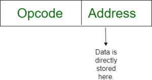
Example: MOV AL, 35H (move the data 35H into AL register)
- Register mode: In register addressing the operand is placed in one of 8 bit or 16 bit general purpose registers. The data is in the register that is specified by the instruction.
Here one register reference is required to access the data.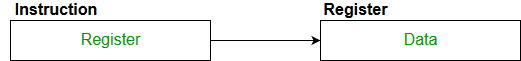
Example: MOV AX,CX (move the contents of CX register to AX register)
- Register Indirect mode: In this addressing the operand’s offset is placed in any one of the registers BX,BP,SI,DI as specified in the instruction. The effective address of the data is in the base register or an index register that is specified by the instruction.
Here two register reference is required to access the data.
The 8086 CPUs let you access memory indirectly through a register using the register indirect addressing modes.MOV AX, [BX](move the contents of memory location s addressed by the register BX to the register AX)
- Auto Indexed (increment mode): Effective address of the operand is the contents of a register specified in the instruction. After accessing the operand, the contents of this register are automatically incremented to point to the next consecutive memory location.(R1)+.
Here one register reference,one memory reference and one ALU operation is required to access the data.
Example:Add R1, (R2)+ // OR R1 = R1 +M[R2] R2 = R2 + d
Useful for stepping through arrays in a loop. R2 – start of array d – size of an element - Auto indexed ( decrement mode): Effective address of the operand is the contents of a register specified in the instruction. Before accessing the operand, the contents of this register are automatically decremented to point to the previous consecutive memory location. –(R1)
Here one register reference,one memory reference and one ALU operation is required to access the data.
- Implied mode:: In implied addressing the operand is specified in the instruction itself. In this mode the data is 8 bits or 16 bits long and data is the part of instruction.Zero address instruction are designed with implied addressing mode.
Example:
Add R1,-(R2) //OR R2 = R2-d R1 = R1 + M[R2]
Auto decrement mode is same as auto increment mode. Both can also be used to implement a stack as push and pop . Auto increment and Auto decrement modes are useful for implementing “Last-In-First-Out” data structures.
- Direct addressing/ Absolute addressing Mode (symbol [ ]): The operand’s offset is given in the instruction as an 8 bit or 16 bit displacement element. In this addressing mode the 16 bit effective address of the data is the part of the instruction.
Here only one memory reference operation is required to access the data.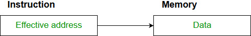
Example:ADD AL,[0301] //add the contents of offset address 0301 to AL
- Indirect addressing Mode (symbol @ or () ):In this mode address field of instruction contains the address of effective address.Here two references are required.
1st reference to get effective address.
2nd reference to access the data.Based on the availability of Effective address, Indirect mode is of two kind:- Register Indirect:In this mode effective address is in the register, and corresponding register name will be maintained in the address field of an instruction.
Here one register reference,one memory reference is required to access the data. - Memory Indirect:In this mode effective address is in the memory, and corresponding memory address will be maintained in the address field of an instruction.
Here two memory reference is required to access the data.
- Register Indirect:In this mode effective address is in the register, and corresponding register name will be maintained in the address field of an instruction.
- Indexed addressing mode: The operand’s offset is the sum of the content of an index register SI or DI and an 8 bit or 16 bit displacement.
Example:MOV AX, [SI +05]
- Based Indexed Addressing: The operand’s offset is sum of the content of a base register BX or BP and an index register SI or DI.
Example: ADD AX, [BX+SI]
- Direct addressing/ Absolute addressing Mode (symbol [ ]): The operand’s offset is given in the instruction as an 8 bit or 16 bit displacement element. In this addressing mode the 16 bit effective address of the data is the part of the instruction.
Based on Transfer of control, addressing modes are:
- PC relative addressing mode: PC relative addressing mode is used to implement intra segment transfer of control, In this mode effective address is obtained by adding displacement to PC.
EA= PC + Address field value PC= PC + Relative value.
- Base register addressing mode: Base register addressing mode is used to implement the inter-segment transfer of control. In this mode effective address is obtained by adding base register value to address field value.
EA= Base register + Address field value. PC= Base register + Relative value.
Note:- PC relative nad based register both addressing modes are suitable for program relocation at runtime.
- Based register addressing mode is best suitable to write position independent codes.
- PC relative addressing mode: PC relative addressing mode is used to implement intra segment transfer of control, In this mode effective address is obtained by adding displacement to PC.
Advantages of Addressing Modes
- To give programmers to facilities such as Pointers, counters for loop controls, indexing of data and program relocation.
- To reduce the number of bits in the addressing field of the Instruction.
Sample GATE Question
Match each of the high-level language statements given on the left-hand side with the most natural addressing mode from those listed on the right-hand side.
1. A[1] = B[J]; a. Indirect addressing 2. while [*A++]; b. Indexed addressing 3. int temp = *x; c. Autoincrement
(A) (1, c), (2, b), (3, a)
(B) (1, a), (2, c), (3, b)
(C) (1, b), (2, c), (3, a)
(D) (1, a), (2, b), (3, c)
(B) (1, a), (2, c), (3, b)
(C) (1, b), (2, c), (3, a)
(D) (1, a), (2, b), (3, c)
Answer: (C)
Explanation:
List 1 List 2 1) A[1] = B[J]; b) Index addressing Here indexing is used 2) while [*A++]; c) auto increment The memory locations are automatically incremented 3) int temp = *x; a) Indirect addressing Here temp is assigned the value of int type stored at the address contained in X
Hence (C) is correct solution.
Hardwired v/s Micro-programmed Control Unit
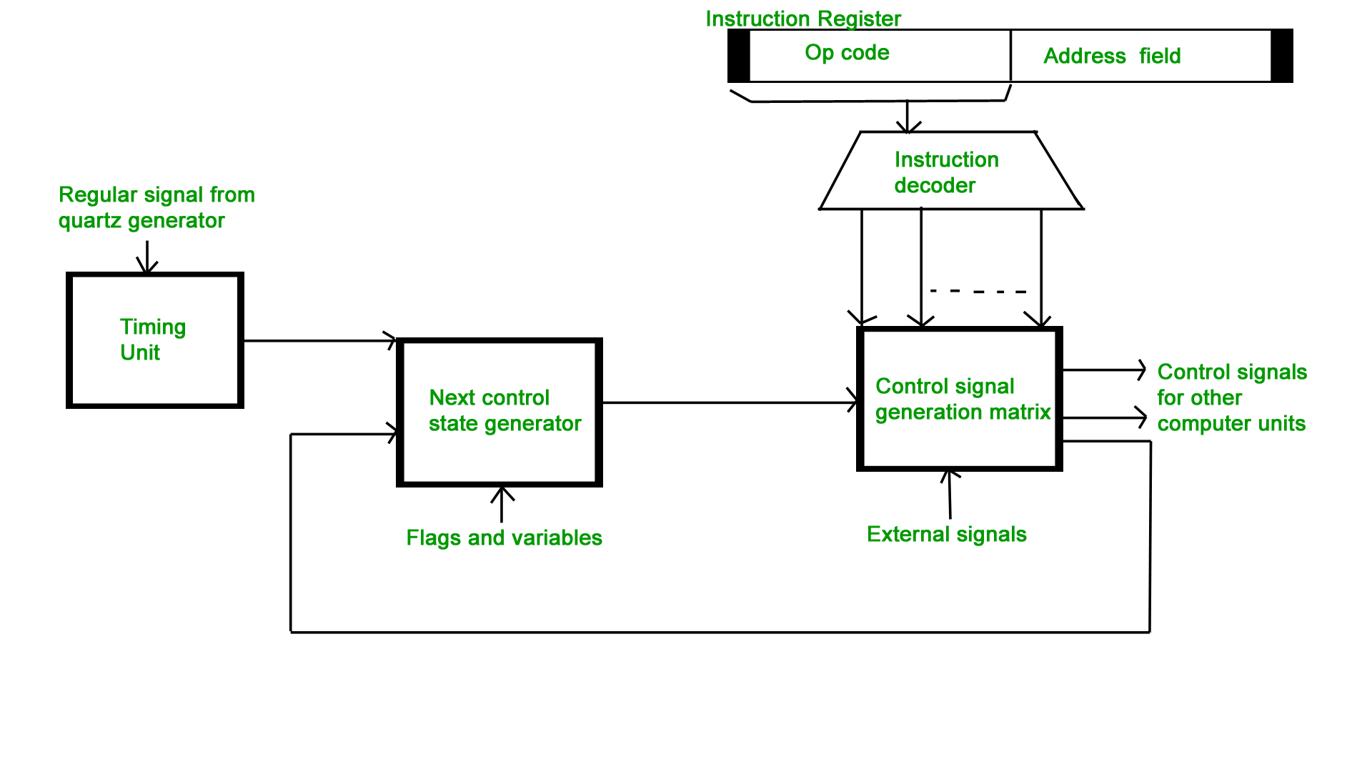
To execute an instruction, the control unit of the CPU must generate the required control signal in the proper sequence. There are two approaches used for generating the control signals in proper sequence as Hardwired Control unit and Micro-programmed control unit.
Hardwired Control Unit –
The control hardware can be viewed as a state machine that changes from one state to another in every clock cycle, depending on the contents of the instruction register, the condition codes, and the external inputs. The outputs of the state machine are the control signals. The sequence of the operation carried out by this machine is determined by the wiring of the logic elements and hence named as “hardwired”.
The control hardware can be viewed as a state machine that changes from one state to another in every clock cycle, depending on the contents of the instruction register, the condition codes, and the external inputs. The outputs of the state machine are the control signals. The sequence of the operation carried out by this machine is determined by the wiring of the logic elements and hence named as “hardwired”.
- Fixed logic circuits that correspond directly to the Boolean expressions are used to generate the control signals.
- Hardwired control is faster than micro-programmed control.
- A controller that uses this approach can operate at high speed.
- RISC architecture is based on a hardwired control unit
s>
Micro-programmed Control Unit –
Micro-programmed Control Unit –
- The control signals associated with operations are stored in special memory units inaccessible by the programmer as Control Words.
- Control signals are generated by a program are similar to machine language programs.
- A micro-programmed control unit is slower in speed because of the time it takes to fetch microinstructions from the control memory.
Some Important Terms –
- Control Word: A control word is a word whose individual bits represent various control signals.
- Micro-routine: A sequence of control words corresponding to the control sequence of a machine instruction constitutes the micro-routine for that instruction.
- Micro-instruction: Individual control words in this micro-routine are referred to as microinstructions.
- Micro-program: A sequence of micro-instructions is called a micro-program, which is stored in a ROM or RAM called a Control Memory (CM).
- Control Store: the micro-routines for all instructions in the instruction set of a computer are stored in a special memory called the Control Store.
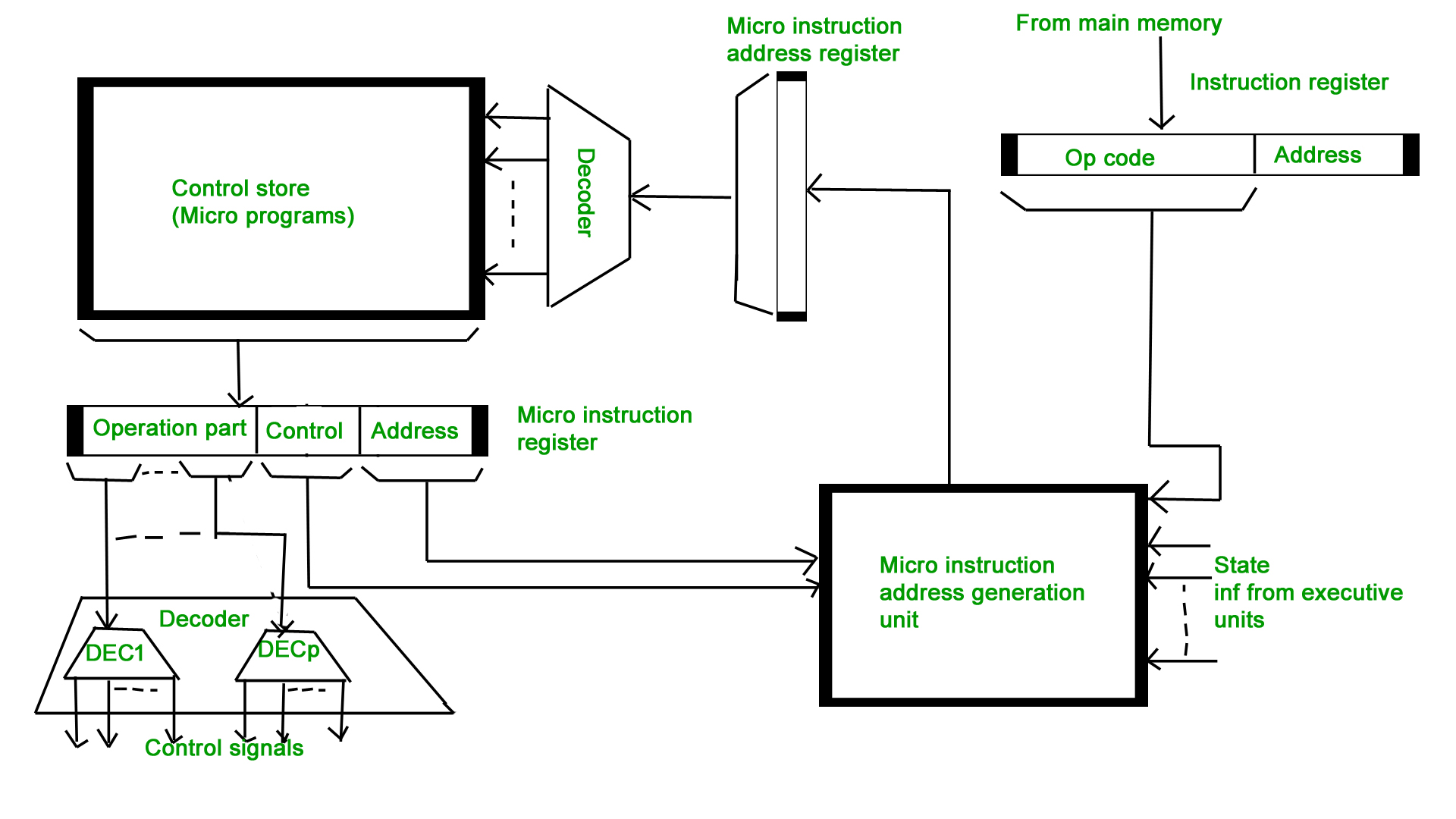
Types of Micro-programmed Control Unit – Based on the type of Control Word stored in the Control Memory (CM), it is classified into two types :
1. Horizontal Micro-programmed Control Unit :
The control signals are represented in the decoded binary format that is 1 bit/CS. Example: If 53 Control signals are present in the processor than 53 bits are required. More than 1 control signal can be enabled at a time.
The control signals are represented in the decoded binary format that is 1 bit/CS. Example: If 53 Control signals are present in the processor than 53 bits are required. More than 1 control signal can be enabled at a time.
- It supports longer control words.
- It is used in parallel processing applications.
- It allows a higher degree of parallelism. If the degree is n, n CS is enabled at a time.
- It requires no additional hardware(decoders). It means it is faster than Vertical Microprogrammed.
- It is more flexible than vertical microprogrammed
2. Vertical Micro-programmed Control Unit :
The control signals re represented in the encoded binary format. For N control signals- Log2(N) bits are required.
The control signals re represented in the encoded binary format. For N control signals- Log2(N) bits are required.
- It supports shorter control words.
- It supports the easy implementation of new control signals, therefore, it is more flexible.
- It allows a low degree of parallelism i.e., the degree of parallelism is either 0 or 1.
- Requires additional hardware (decoders) to generate control signals, it implies it is slower than horizontal microprogrammed.
- It is less flexible than horizontal but more flexible than that of the hardwired control unit.
GATE CS Corner Questions
Practicing the following questions will help you test your knowledge. All questions have been asked in GATE in previous years or in GATE Mock Tests. It is highly recommended that you practice them.
Practicing the following questions will help you test your knowledge. All questions have been asked in GATE in previous years or in GATE Mock Tests. It is highly recommended that you practice them.
RISC and CISC
Reduced Set Instruction Set Architecture (RISC) –
The main idea behind is to make hardware simpler by using an instruction set composed of a few basic steps for loading, evaluating and storing operations just like a load command will load data, store command will store the data.
The main idea behind is to make hardware simpler by using an instruction set composed of a few basic steps for loading, evaluating and storing operations just like a load command will load data, store command will store the data.
Complex Instruction Set Architecture (CISC) –
The main idea is to make hardware complex as a single instruction will do all loading, evaluating and storing operations just like a multiplication command will do stuff like loading data, evaluating and storing it.
The main idea is to make hardware complex as a single instruction will do all loading, evaluating and storing operations just like a multiplication command will do stuff like loading data, evaluating and storing it.
Both approaches try to increase the CPU performance
- RISC: Reduce the cycles per instruction at the cost of the number of instructions per program.
- CISC: The CISC approach attempts to minimize the number of instructions per program but at the cost of increase in number of cycles per instruction.
Earlier when programming was done using assembly language, a need was felt to make instruction do more task because programming in assembly was tedious and error prone due to which CISC architecture evolved but with uprise of high level language dependency on assembly reduced RISC architecture prevailed.
Characteristic of RISC –
- Simpler instruction, hence simple instruction decoding.
- Instruction come under size of one word.
- Instruction take single clock cycle to get executed.
- More number of general purpose register.
- Simple Addressing Modes.
- Less Data types.
- Pipeling can be achieved.
Characteristic of CISC –
- Complex instruction, hence complex instruction decoding.
- Instruction are larger than one word size.
- Instruction may take more than single clock cycle to get executed.
- Less number of general purpose register as operation get performed in memory itself.
- Complex Addressing Modes.
- More Data types.
Example – Suppose we have to add two 8-bit number:
- CISC approach: There will be a single command or instruction for this like ADD which will perform the task.
- RISC approach: Here programmer will write first load command to load data in registers then it will use suitable operator and then it will store result in desired location.
So, add operation is divided into parts i.e. load, operate, store due to which RISC programs are longer and require more memory to get stored but require less transistors due to less complex command.
Difference –
| RISC | CISC |
|---|---|
| Focus on software | Focus on hardware |
| Transistors are used for more registers | Transistors are used for storing complex Instructions |
| Code size is large | Code size is small |
| A instruction execute in single clock cycle | Instruction take more than one clock cycle |
| A instruction fit in one word | Instruction are larger than size of one word |
Memory Hierarchy
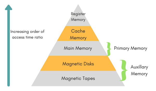
The total memory capacity of a computer can be visualized by hierarchy of components. The memory hierarchy system consists of all storage devices contained in a computer system from the slow Auxiliary Memory to fast Main Memory and to smaller Cache memory.
Auxillary memory access time is generally 1000 times that of the main memory, hence it is at the bottom of the hierarchy.
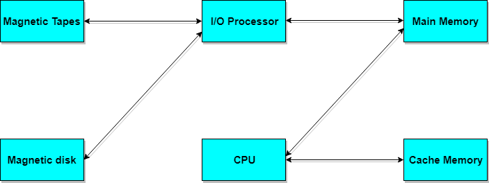
The main memory occupies the central position because it is equipped to communicate directly with the CPU and with auxiliary memory devices through Input/output processor (I/O).
When the program not residing in main memory is needed by the CPU, they are brought in from auxiliary memory. Programs not currently needed in main memory are transferred into auxiliary memory to provide space in main memory for other programs that are currently in use.
The cache memory is used to store program data which is currently being executed in the CPU. Approximate access time ratio between cache memory and main memory is about 1 to 7~10
Memory Access Methods
Each memory type, is a collection of numerous memory locations. To access data from any memory, first it must be located and then the data is read from the memory location. Following are the methods to access information from memory locations:
- Random Access: Main memories are random access memories, in which each memory location has a unique address. Using this unique address any memory location can be reached in the same amount of time in any order.
- Sequential Access: This methods allows memory access in a sequence or in order.
- Direct Access: In this mode, information is stored in tracks, with each track having a separate read/write head.
Main Memory
The memory unit that communicates directly within the CPU, Auxillary memory and Cache memory, is called main memory. It is the central storage unit of the computer system. It is a large and fast memory used to store data during computer operations. Main memory is made up of RAM and ROM, with RAM integrated circuit chips holing the major share.
- RAM: Random Access Memory
- DRAM: Dynamic RAM, is made of capacitors and transistors, and must be refreshed every 10~100 ms. It is slower and cheaper than SRAM.
- SRAM: Static RAM, has a six transistor circuit in each cell and retains data, until powered off.
- NVRAM: Non-Volatile RAM, retains its data, even when turned off. Example: Flash memory.
- ROM: Read-Only Memory, is non-volatile and is more like permanent storage for information. It also stores the bootstrap loader program, to load and start the operating system when computer is turned on. PROM(Programmable ROM), EPROM(Erasable PROM) and EEPROM(Electrically Erasable PROM) are some commonly used ROMs.
Auxiliary Memory
Devices that provide backup storage are called auxiliary memory. For example: Magnetic disks and tapes are commonly used auxiliary devices. Other devices used as auxiliary memory are magnetic drums, magnetic bubble memory and optical disks.
It is not directly accessible to the CPU, and is accessed using the Input/Output channels.
Cache Memory
The data or contents of the main memory that are used again and again by CPU, are stored in the cache memory so that we can easily access that data in shorter time.
Whenever the CPU needs to access memory, it first checks the cache memory. If the data is not found in cache memory then the CPU moves onto the main memory. It also transfers block of recent data into the cache and keeps on deleting the old data in cache to accomodate the new one.
Hit Ratio
The performance of cache memory is measured in terms of a quantity called hit ratio. When the CPU refers to memory and finds the word in cache it is said to produce a hit. If the word is not found in cache, it is in main memory then it counts as a miss.
The ratio of the number of hits to the total CPU references to memory is called hit ratio.
Hit Ratio = Hit/(Hit + Miss)Associative Memory
It is also known as content addressable memory (CAM). It is a memory chip in which each bit position can be compared. In this the content is compared in each bit cell which allows very fast table lookup. Since the entire chip can be compared, contents are randomly stored without considering addressing scheme. These chips have less storage capacity than regular memory chips.
Comments
Post a Comment